We work with leading brands, retailers and operators to engage customers using the latest technology and deliver seamless retail experiences they won’t forget.
OUR divisions
Explore our full automated retail range from digital vending solutions to micro-markets, coffee-to-go to smart fridges and freezers.
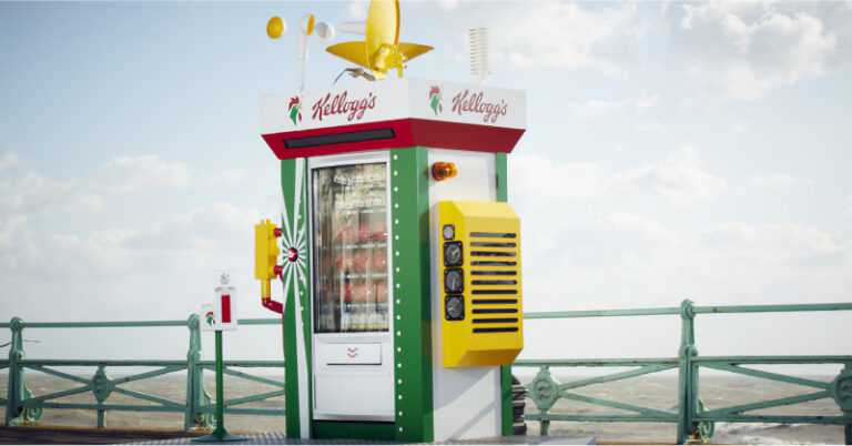
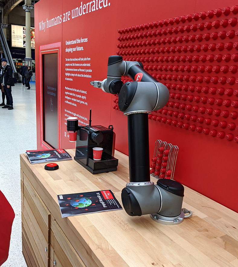
We bring together cutting-edge technologies to create and deliver ‘phygital’ experiences that wow consumers in new and memorable ways.
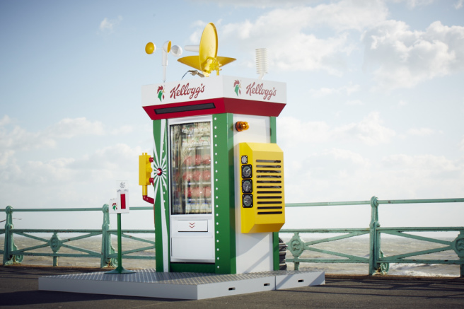
We’re passionate about creating disruptive products – from new vending concepts, through to eco-sustainable dispensing solutions for a plastic free world.
OUR Technology
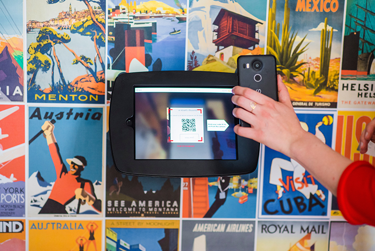
Providing advanced telemetry data, content management, promotional capabilities and detailed analytics for any retail device, anywhere.
Go to Vendlive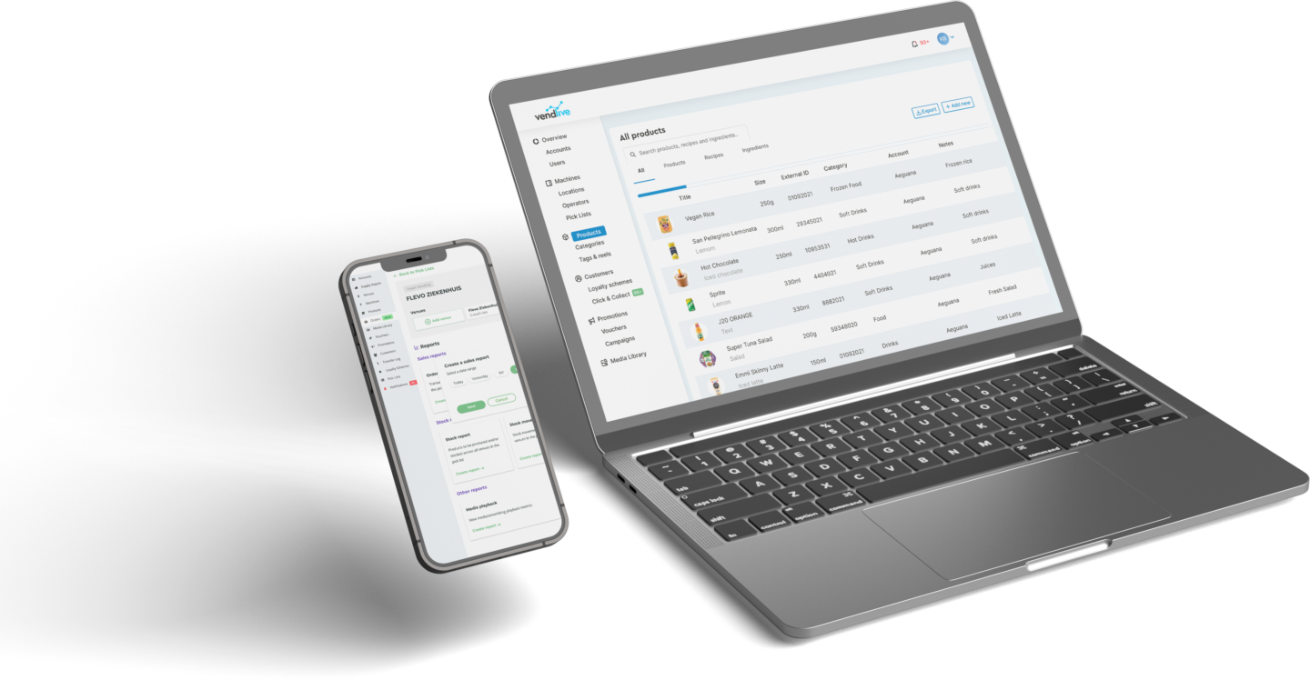
The world’s most advanced automated retail technology
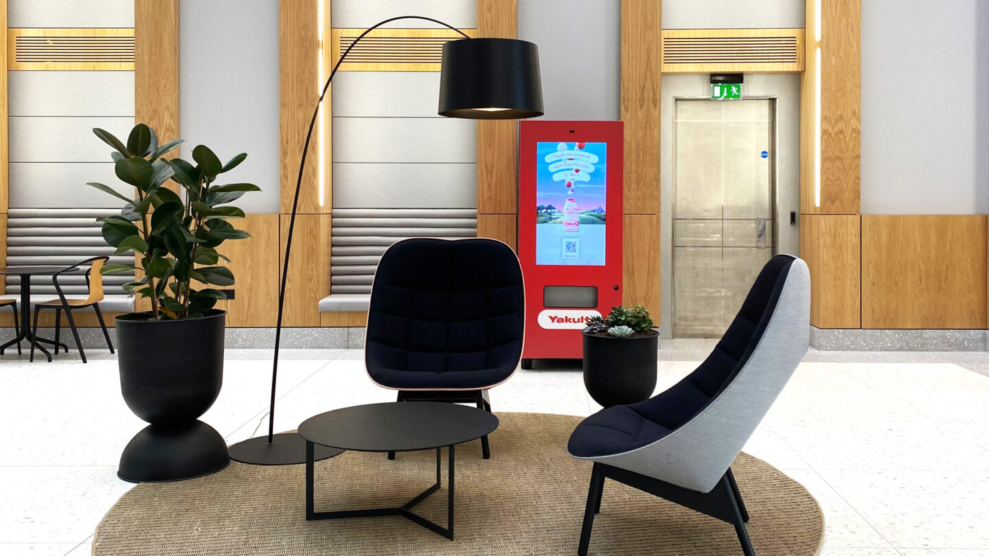
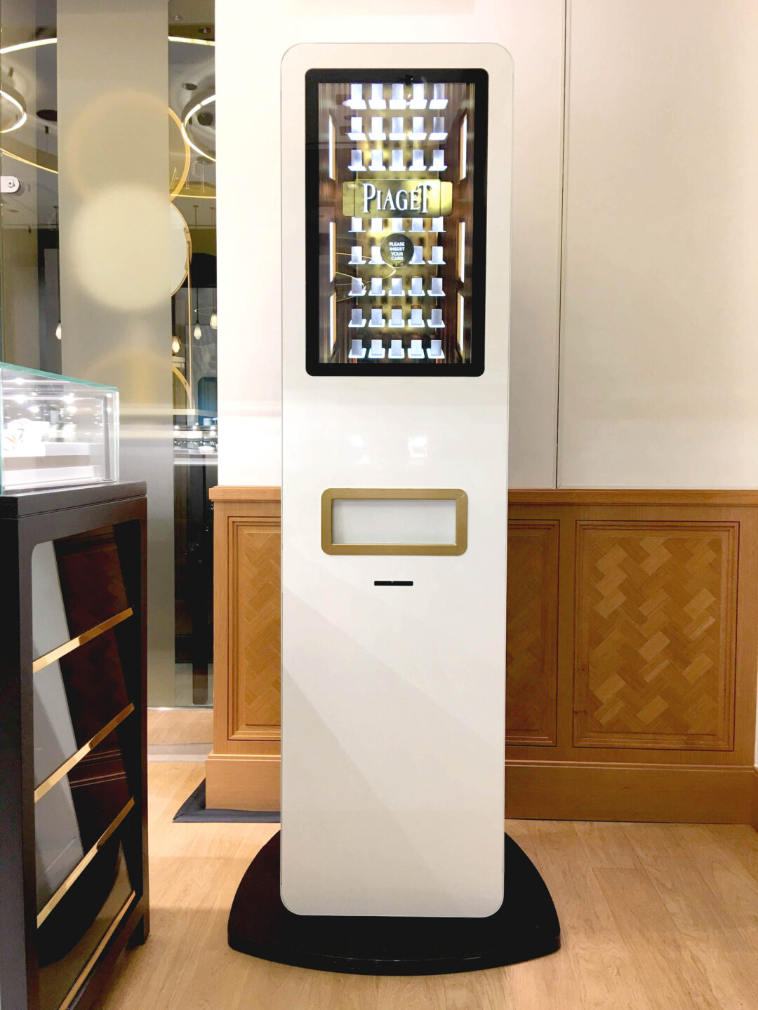
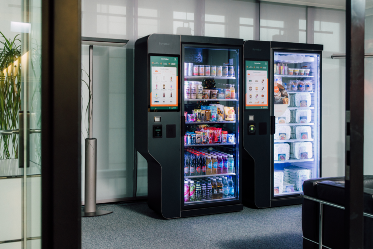
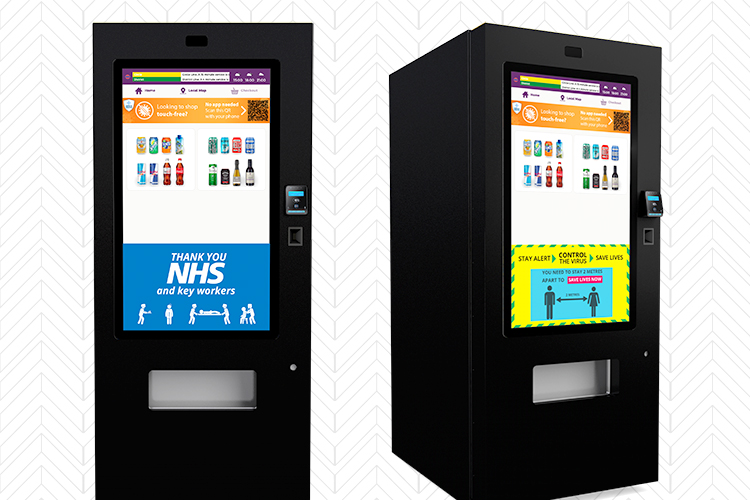
Digital vending machines designed for high throughput locations including fresh food & high value items.
Explore the range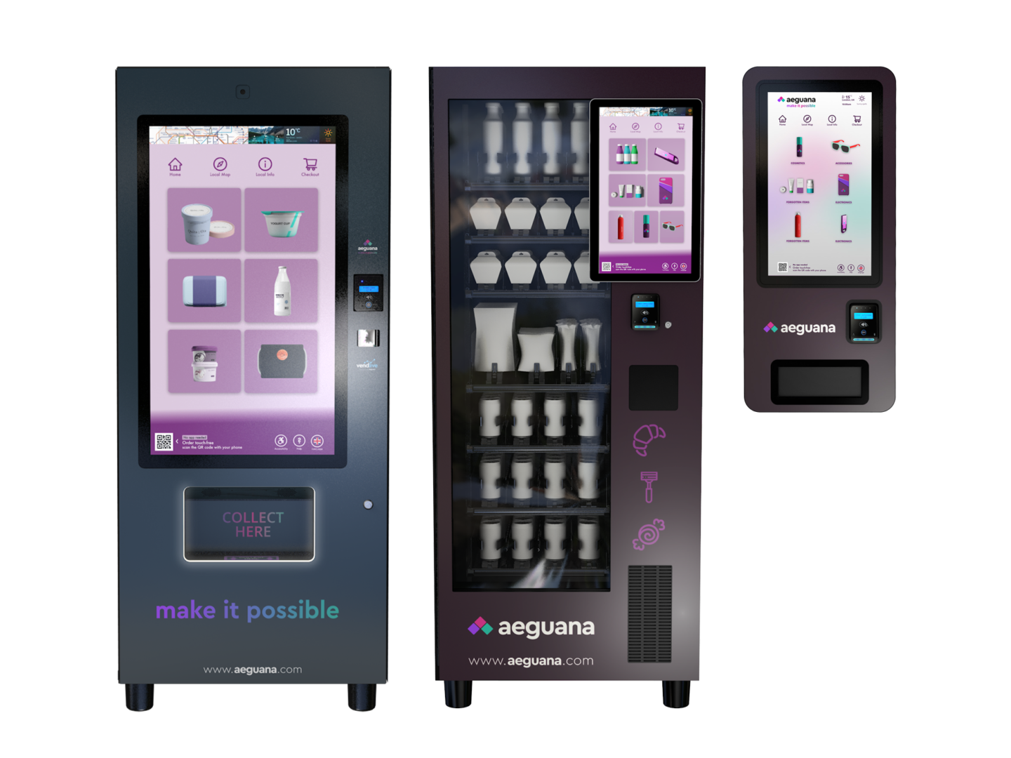
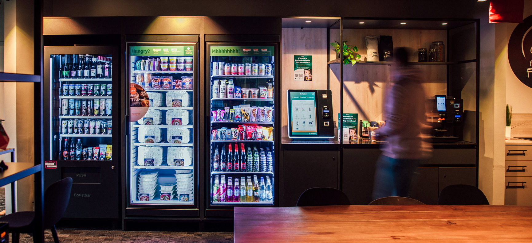
Micro Market solutions with a difference. Combine our EPOS with any of our vending machines, fridges, freezers or coffee units to create a unique, modular Micro Market offering.
Explore the range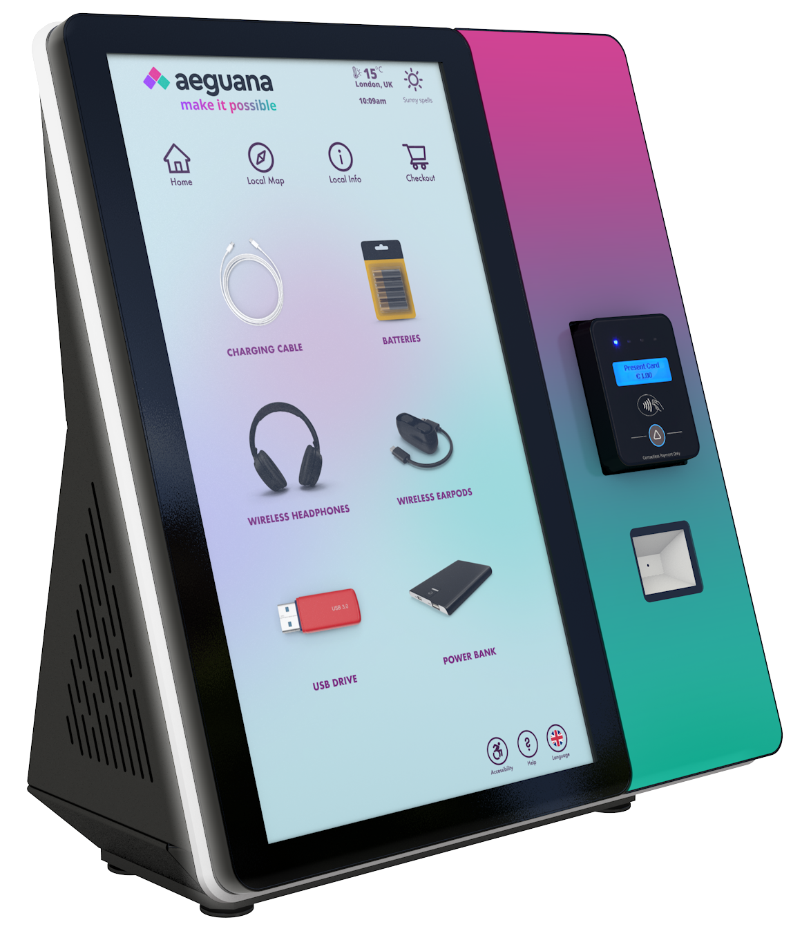
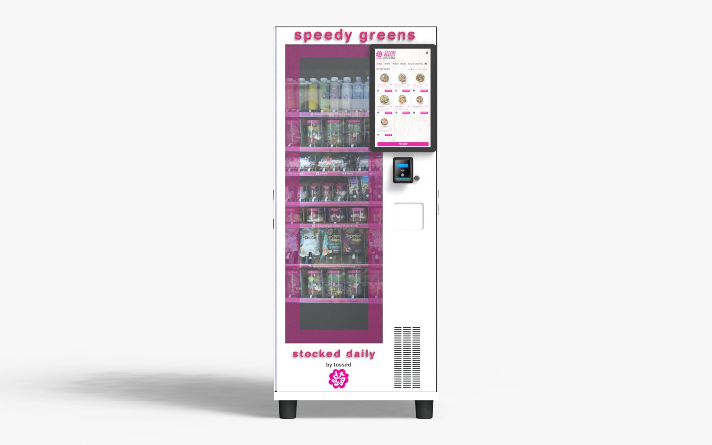
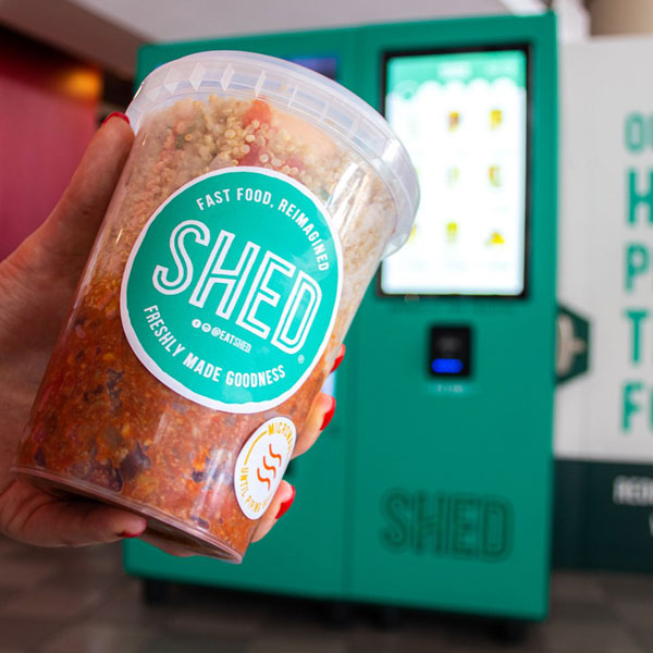
A seamless buying experience designed for fresh food, snacks, and frozen meals. Truly “grab & go” retail, powered by cutting edge technology.
Explore the range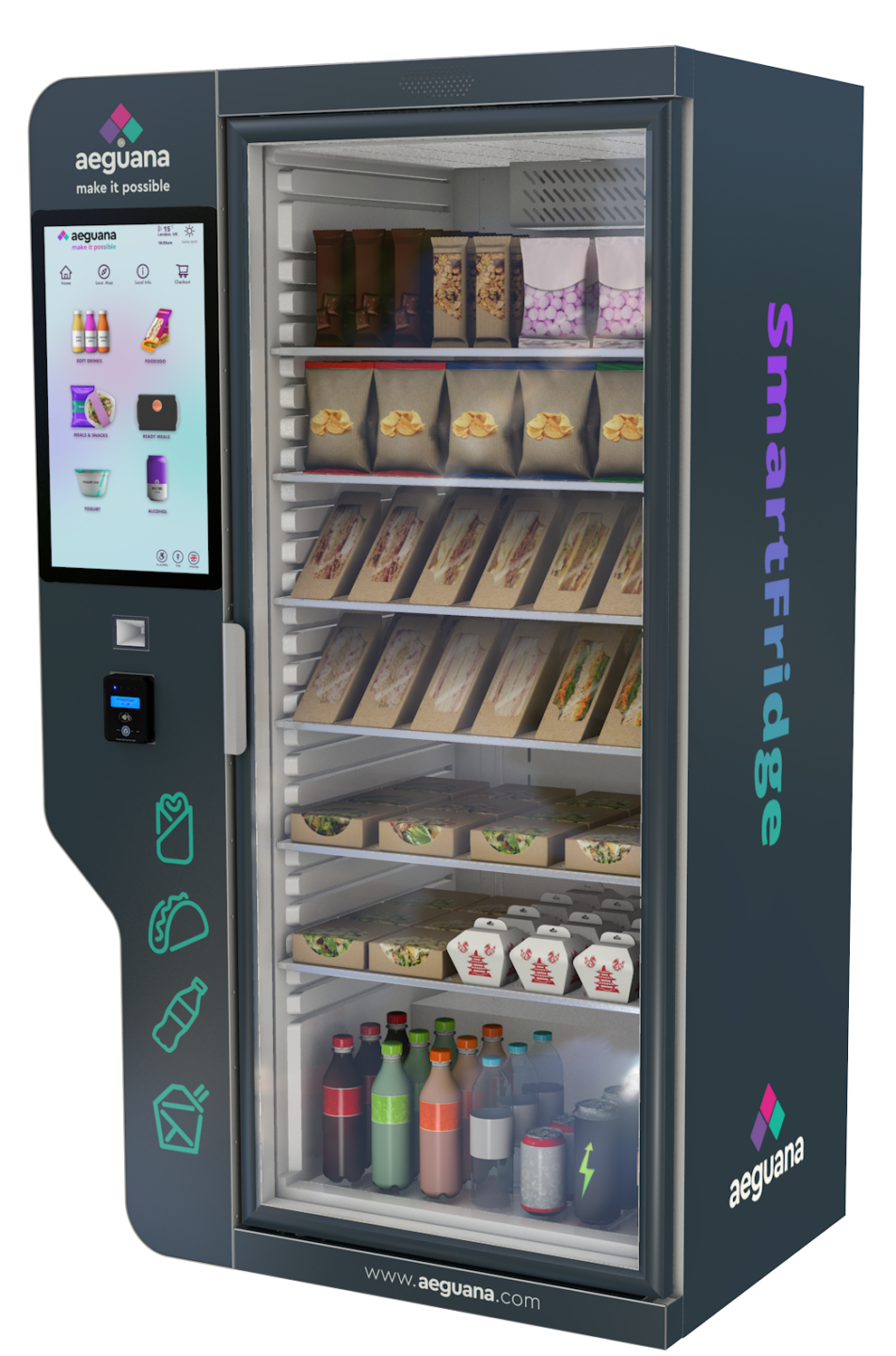
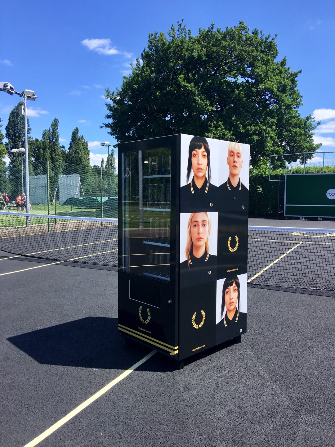
Digital freestanding and table top coffee units from leading global manufacturers, integrated with just about everything. Personalise drinks. Reward consumers. Enjoy.
Explore the range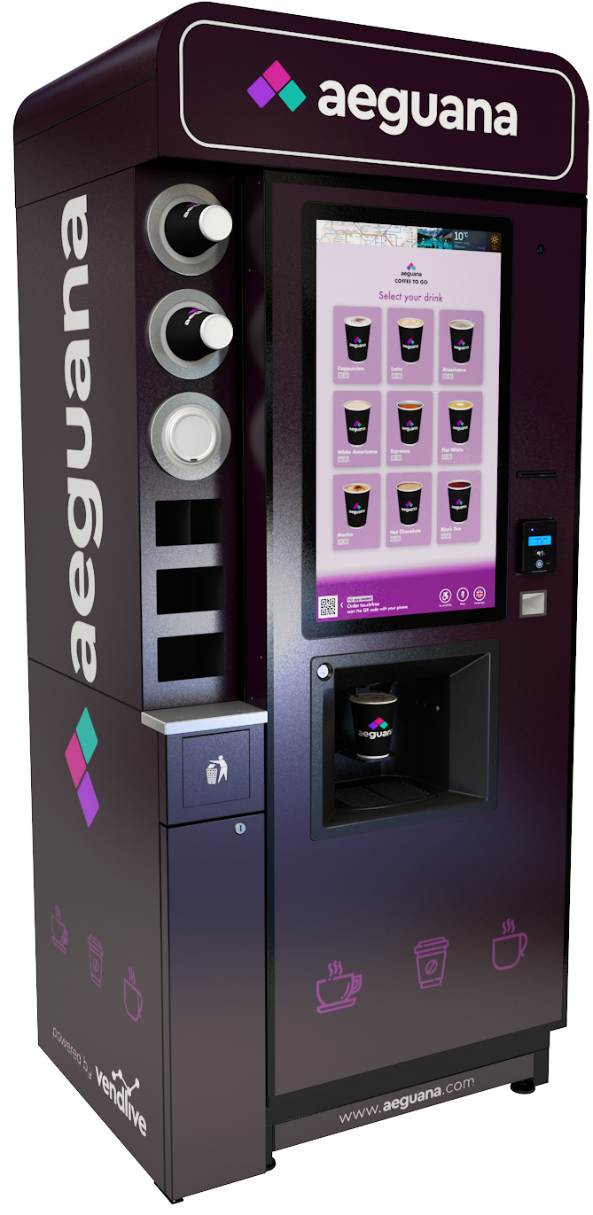
The world’s most advanced automated retail technology
Our customers are redefining vending


"Aeguana are the best agency I have ever worked with. What they produce is startlingly good and the service they provide is fantastic.”
"Jason and the team are true experts and market leaders when it comes to all things Vending. If you're looking to create an engaging experience for customers, look no further than Aeguana."
"I have known most of the team at Aeguana for many years, and have seen them grow into highly specialised individuals. They know they're stuff."
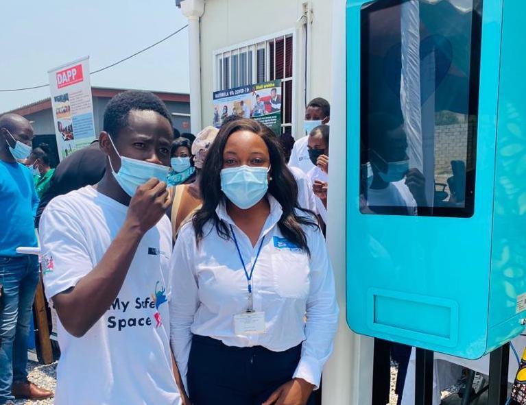
Vendies innovation award – Touch-free technology in an era of COVID-19.
Vendies innovation in sustainability award in partnership with Sipple

British Engineering Excellence Award

Aeguana was shortlisted for the Technology Innovation award.


Read more
Read more
Read more
Read more
Read more
Read more
Our intelligent vending machines operate seamlessly across the globe, interacting with VendLive, and delivering products to happy customers everywhere.
Can’t call us right now? That’s ok. Use our form and we’ll get back to you within 24 hours.
"*" indicates required fields